Citations
Study of the influence of indium segregation and Internal electric-field on the optical properties of III-V quantum wells heterostructures
Estudio de la influencia de la segregación de indio y del campo eléctrico interno en las propiedades ópticas de heteroestructuras de pozos cuánticos III-V
Open | Download
Issue
Section
Articles
How to Cite
Study of the influence of indium segregation and Internal electric-field on the optical properties of III-V quantum wells heterostructures. (2021). Revista EIA, 18(36), 36020 pp. 1-14. https://doi.org/10.24050/reia.v18i36.1511
Dimensions


license

This work is licensed under a Creative Commons Attribution-NonCommercial-NoDerivatives 4.0 International License.
Copyright statement
The authors exclusively assign to the Universidad EIA, with the power to assign to third parties, all the exploitation rights that derive from the works that are accepted for publication in the Revista EIA, as well as in any product derived from it and, in in particular, those of reproduction, distribution, public communication (including interactive making available) and transformation (including adaptation, modification and, where appropriate, translation), for all types of exploitation (by way of example and not limitation : in paper, electronic, online, computer or audiovisual format, as well as in any other format, even for promotional or advertising purposes and / or for the production of derivative products), for a worldwide territorial scope and for the entire duration of the rights provided for in the current published text of the Intellectual Property Law. This assignment will be made by the authors without the right to any type of remuneration or compensation.
Consequently, the author may not publish or disseminate the works that are selected for publication in the Revista EIA, neither totally nor partially, nor authorize their publication to third parties, without the prior express authorization, requested and granted in writing, from the Univeridad EIA.
Show authors biography


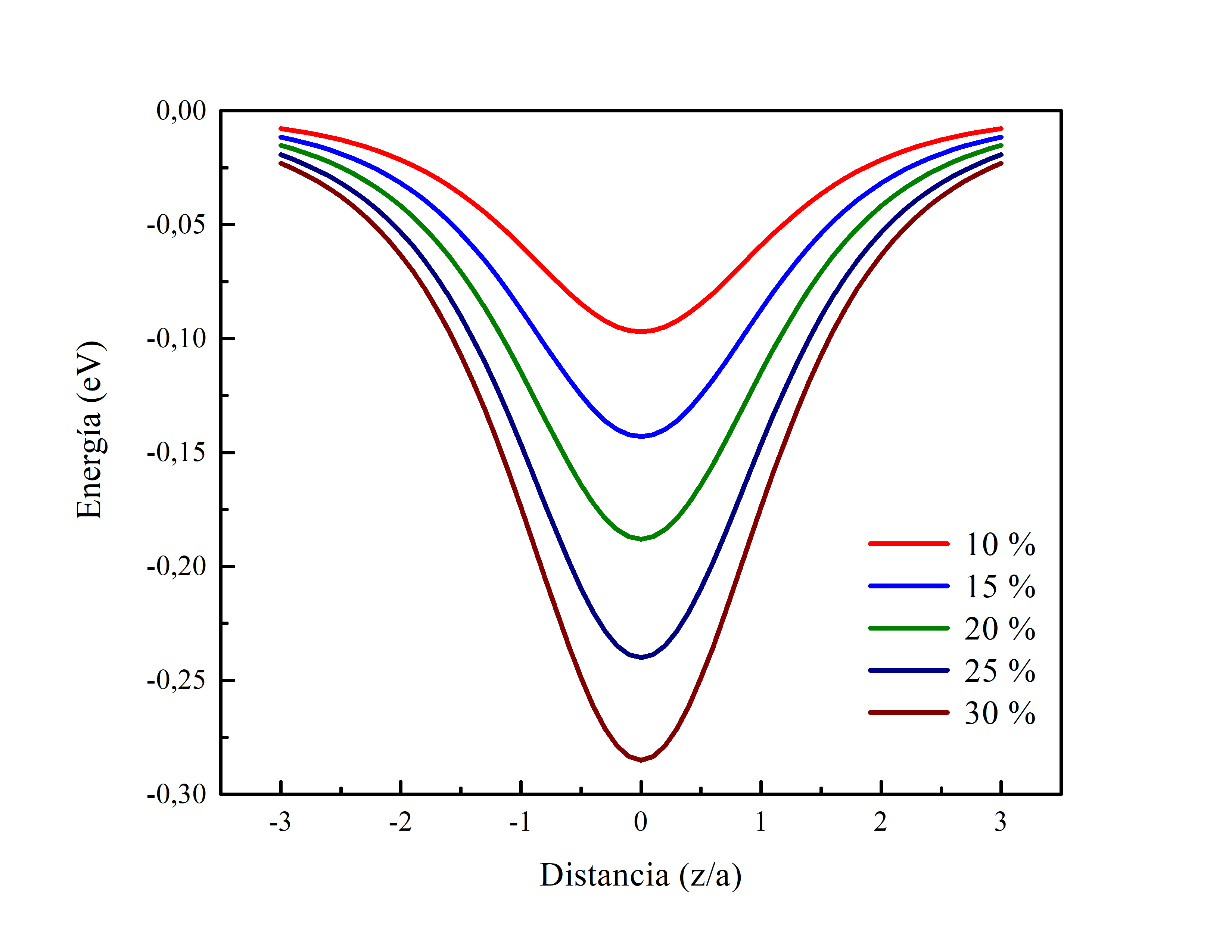
The surface segregation in III-V semiconductor alloys produce abrupt interfaces, and modifies the potential profiles, alternating the electronic states in the quantum well and the emission energy in the photoluminescence spectrum. In this work, the Schrödinger equation is solved by means of a power series considering a Cauchy type symmetrical potential, which is soft and decreasing to infinity. This potential is proposed due to the changes in the potential profile from quantum well by the segregation of atoms during the growth process. The ground state energy was determined according to the parameters that characterize this potential. This model was applied to the particular case of indium segregation in the InGaAs/GaAs system. The ground state energy transition is calculated from the difference in energy between the electron and hole in function of well width. These calculations are in agreement with the reported photoluminescence peak energies. In addition, the influence of the electrical field due to the piezoelectric effect on the photoluminescence emission is studied. For this purpose, an electron variational wavefunction was considered and the ground state energy transition in the active region of the heterostructure was calculated from the difference in energy between the electron and hole in function of well width and the electric field. For InGaAs/GaAs quantum wells, the ground energy is adjusted within this model coinciding our theoretical calculations with the experimental part.
Article visits 503 | PDF visits 193
Downloads
Download data is not yet available.
- Ahn, D.; Chuang, S. L. (1986). Variational calculations of subbands in a quantum well with uniform electric field: Gram–Schmidt orthogonalization approach. Applied Physics Letters, 49(21), pp. 1450–1452. https://doi.org/10.1063/1.97299
- Bastard, G.; Mendez, E. E.; Chang, L. L.; Esaki, L. (1983). Variational calculations on a quantum well in an electric field. Physical Review B, 28(6), pp. 3241–3245. https://doi.org/10.1103/PhysRevB.28.3241
- Bonef, B.; Catalano, M.; Lund, C.; Denbaars, S. P.; Nakamura, S.; Mishra, U. K.; Kim, M. J.; Keller, S. (2017). Indium segregation in N-polar InGaN quantum wells evidenced by energy dispersive X-ray spectroscopy and atom probe tomography. Applied Physics Letters, 110(14), pp. 143101. https://doi.org/10.1063/1.4979786
- Chan, C. H.; Chen, Y. F.; Chen, M. C.; Lin, H. H.; Jan, G. J.; Chen, Y. H. (1998). Photoreflectance spectroscopy of strained-layer (111)B InGaAs/GaAs quantum well diodes. Journal of Applied Physics, 84(3), pp. 1595–1601. https://doi.org/10.1063/1.368229
- Chenini, L.; Aissat, A.; Ammi, S.; Vilcot, J. P. (2021). Investigation of temperature, well width and composition effects on the intersubband absorption of InGaAs/GaAs quantum wells. Lecture Notes in Electrical Engineering, 681, pp. 325–332. https://doi.org/10.1007/978-981-15-6259-4_34
- Deng, Z.; Jiang, Y.; Wang, W.; Cheng, L.; Li, W.; Lu, W.; Jia, H.; Liu, W.; Zhou, J.; Chen, H. (2014). Indium segregation measured in InGaN quantum well layer. Scientific Reports, 4, pp. 6734. https://doi.org/10.1038/srep06734
- Dickey, S. A.; Majerfeld, A.; Sánchez-Rojas, J. L.; Sacedón, A.; Muñoz, E.; Sanz-Hervás, A.; Aguilar, M.; Kim, B. W. (1998). Direct determination of the piezoelectric field in (111) strained InGaAs/GaAs multiple quantum well p-i-n structures by photoreflectance. Microelectronic Engineering, 43–44, pp. 171–177. https://doi.org/10.1016/S0167-9317(98)00160-9
- Dong, H.; Sun, J.; Ma, S.; Liang, J.; Lu, T.; Liu, X.; Xu, B. (2016). Influence of substrate misorientation on the photoluminescence and structural properties of InGaAs/GaAsP multiple quantum wells. Nanoscale, 8(11), pp. 6043–6056. https://doi.org/10.1039/C5NR07938A
- G. Gonzalez de la Cruz. (2004). The Influence of surface segregation on the optical properties of semiconductor quantum wells. Journal of Applied Physics, 96(7), pp. 3752–3755. https://doi.org/DOI: 10.1063/1.1789628
- Gonzalez de la Cruz, G.; Arenas, A. C.; Herrera, H. (2005). Internal electric-field and segregation effects on luminescence properties of quantum wells. Journal of Applied Physics, 98(2). https://doi.org/10.1063/1.1954889
- Hiyamizu, S.; Ohno, Y.; Higashiwaki, M.; Shimomura, S. (1999). In0.15Ga0.85As/GaAs quantum wire structures grown on (553)B GaAs substrates by molecular beam epitaxy. Journal of Crystal Growth, 201(202), pp. 824–827.
- Loykaew, A.; Usher, B. F.; Jones, R. T.; Pigram, P. J. (2013). A Novel Sample Structure for the Measurement of Indium Segregation Profiles in GaAs/InGaAs/GaAs Heterostructures. International Journal of Applied Physics and Mathematics, 3(3), pp. 191–197. https://doi.org/10.7763/IJAPM.2013.V3.204
- Martínez-Rendón, V.; Castaño-Uribe, C.; Giraldo-Martínez, A.; González-Pereira, J. P.; Restrepo-Arango, R. L.; Morales-Armburu, Á. L.; Duque-Echeverri, C. A. (2016). Potencial de Morse como perfil de pozos cuánticos semiconductores. Revista EIA, 12(3), pp. 85–94. https://doi.org/10.24050/reia.v12i2.966
- Martini, S.; Manzoli, J. E.; Quivy, A. A. (2010). Study of the influence of indium segregation on the optical properties of InGaAs/GaAs quantum wells via split-operator method. Journal of Vacuum Science & Technology B, Nanotechnology and Microelectronics: Materials, Processing, Measurement, and Phenomena, 28(2), pp. 277–283. https://doi.org/10.1116/1.3301612
- Massabuau, F. C.-P.; Rhode, S. L.; Horton, M. K.; O’Hanlon, T. J.; Kovács, A.; Zielinski, M. S.; Kappers, M. J.; Dunin-Borkowski, R. E.; Humphreys, C. J.; Oliver, R. A. (2017). Dislocations in AlGaN: Core Structure, Atom Segregation, and Optical Properties. Nano Letters, 17(8), pp. 4846–4852. https://doi.org/10.1021/acs.nanolett.7b01697
- Mehrtens, T.; Müller, K.; Schowalter, M.; Hu, D.; Schaadt, D. M.; Rosenauer, A. (2013). Measurement of indium concentration profiles and segregation efficiencies from high-angle annular dark field-scanning transmission electron microscopy images. Ultramicroscopy, 131, pp. 1–9. https://doi.org/10.1016/j.ultramic.2013.03.018
- Muraki, K.; Fukatsu, S.; Shiraki, Y. (1992). :Surface segregation of In atoms during molecular beam epitaxy and its influence on the energy levels in InGaAs/GaAs quantum wells. Applied Physics Letters, 61(5), pp. 10.1063/1.107835.
- Muraki, K.; Fukatsu, S.; Shiraki, Y.; Ito, R. (1992). Surface segregation of In atoms during molecular beam epitaxy and its influence on the energy levels in InGaAs/GaAs quantum wells. Applied Physics Letters, 61(5), pp. 557–559. https://doi.org/10.1063/1.107835
- Rojas-Ramírez, J. S.; Goldhahn, R.; Moser, P.; Huerta-Ruelas, J.; Hernández-Rosas, J.; López-López, M. (2008). Temperature dependence of the photoluminescence emission from InxGa1-xAs quantum wells on GaAs(311) substrates. Journal of Applied Physics, 104(12), pp. 1–6. https://doi.org/10.1063/1.3043578
- Schowalter, M.; Rosenauer, A.; Gerthsen, D. (2006). Influence of surface segregation on the optical properties of semiconductor quantum wells. Applied Physics Letters, 88(11), pp. 111906. https://doi.org/10.1063/1.2184907
- Shan, R.; Liu, Y.; Guo, J.; Wang, G.; Xu, Y. (2016). Growth and characterization of high strain InGaAs/GaAs quantum well by molecular beam epitaxy. 10157, pp. 101573F. https://doi.org/10.1117/12.2247398
- Smith, D. L.; Mailhiot, C. (1988). Piezoelectric effects in strained‐layer superlattices. Journal of Applied Physics, 63(8), pp. 2717–2719. https://doi.org/10.1063/1.340965
- Song, K.-M.; Kim, J.-M.; Kang, B.-K.; Yoon, D.-H.; Kang, S.; Lee, S.-W.; Lee, S.-N. (2012). Characteristics of indium incorporation in InGaN/GaN multiple quantum wells grown on a-plane and c-plane GaN. Applied Physics Letters, 100(21), pp. 212103. https://doi.org/10.1063/1.4720507
- Srinivasan, T.; Muralidharan, R.; Mehta, S. K.; Jain, B. P.; Singh, S. N.; Jain, R. K.; Kumar, V. (2001). Characterisation of molecular beam epitaxy-grown InGaAs multilayer structures using photoluminescence. Vacuum, 60(4), pp. 425–429. https://doi.org/10.1016/S0042-207X(00)00223-2
- Sun, D.; Towe, E. (1994). Strain-Generated Internal Fields in Pseudomorphic (In, Ga)As/GaAs Quantum Well Structures on {11l} GaAs Substrates. Japanese Journal of Applied Physics, 33(Part 1, No. 1B), pp. 702–708. https://doi.org/10.1143/JJAP.33.702
- Vurgaftman, I.; Meyer, J. R.; Ram-Mohan, L. R. (2001). Band parameters for III-V compound semiconductors and their alloys. Journal of Applied Physics, 89(11 I), pp. 5815–5875. https://doi.org/10.1063/1.1368156
- Wu, S.; Huang, Z.; Liu, Y.; Huang, Q.; Guo, W.; Cao, Y. (2009a). The effects of indium segregation on the valence band structure and optical gain of GaInAs/GaAs quantum wells. Physica E: Low-Dimensional Systems and Nanostructures, 41(9), pp. 1656–1660. https://doi.org/10.1016/j.physe.2009.05.019
- Wu, S.; Huang, Z.; Liu, Y.; Huang, Q.; Guo, W.; Cao, Y. (2009b). The effects of indium segregation on exciton binding energy and oscillator strength in GaInAs/GaAs quantum wells. Superlattices and Microstructures, 46(4), pp. 618–626. https://doi.org/10.1016/j.spmi.2009.06.001
- Yildirim, H.; Tomak, M. (2006). Optical absorption of a quantum well with an adjustable asymmetry. The European Physical Journal B, 50(4), pp. 559–564. https://doi.org/10.1140/epjb/e2006-00182-1